And the U.S. Engineering Powerhouses Driving the Build
By the Resource Erectors Research Team
If you want to know what this July’s hot topic among heavy industry investors and engineering executives is right now, look no further than Nasdaq. South Korea’s semiconductor titan, SK Hynix, just completed a historic Wall Street debut.
The company commands a staggering 56% of the global AI chip market. It shattered IPO records with a colossal $26.5 billion U.S. ADR listing (NASDAQ: SKHY). The IPO price rocketed 13% in its opening hours, all fueled by the world’s insatiable, high-octane demand for AI hardware.
While the finance world watches the stock tickers blink, the real boots-on-the-ground engineering story is unfolding in the dirt of the American Midwest. SK Hynix has officially cleared its initial foundational hurdles.
Backed by urgent calls from the U.S. Department of Commerce to localize microchip production, the company is moving directly into the vertical construction phase, right here on U.S. soil.
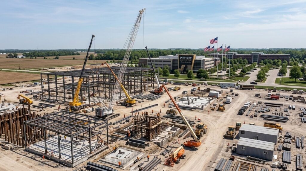
This isn’t just another manufacturing plant. It’s a jaw-dropping $3.87 billion advanced packaging fabrication and R&D facility. The development spans a massive 133.5-acre site within the Purdue Research Park in West Lafayette, Indiana.
In essence, this project marks the return of essential high-tech infrastructure to U.S. soil. For heavy industry, civil engineering, and construction sectors, this build stands as a masterclass in massive domestic engineering mobilization, federal policy alignment, and structural risk mitigation.
SK Hynix, Nvidia, and Taiwan Semiconductor Are Closing the “Advanced Packaging” Critical Gap by Building Here in the US
To understand why the SK Hynix Indiana facility is a complete game-changer, you have to look beyond raw silicon wafer fabrication. The United States has aggressively expanded its capability to design microchips and bake the underlying wafers. Yet, a major, glaring supply chain vulnerability remained:
Advanced Packaging and High-Bandwidth Memory (HBM).
Think of advanced packaging as the hyper-precise, microscopic art of stacking layers of High-Bandwidth Memory directly onto logic processors. This vertical stacking is what builds the high-horsepower Graphics Processing Units (GPUs) required to train modern artificial intelligence models.
Industry giants like Nvidia and Intel frequently tout homegrown American chip supply chain prowess as the country bolsters local production, but critical gaps remain. Even as domestic fabrication projects grow in scope and scale, crucial backend packaging steps for frontline hardware remain stubbornly offshore. This includes work for Nvidia’s powerhouse Blackwell graphics architecture.
Historically, almost 100% of this delicate, microscopic stacking process occurred overseas.
According to the official project outline from the National Institute of Standards and Technology (NIST), the West Lafayette facility will house the first advanced semiconductor packaging line of its scale in the United States. This effectively short-circuits a major geopolitical vulnerability, allowing end-to-end chip capabilities to be delivered entirely on U.S. soil.
Now, let’s take a look at the US companies that have boots on the ground in that Indiana soil…
The U.S. Engineering Powerhouses Driving the Build
Executing a highly sensitive $3.87 billion facility requires hyper-controlled cleanroom environments, massive ultra-pure water systems, and structural tolerances that leave absolute zero room for error. To bring this facility to life by its mass-production target in the second half of 2028, a premier roster of American civil, structural, and mechanical engineering firms is driving the day-to-day progress:
Hi-Tech Engineering Partners
This is the U.S. subsidiary of SK Hynix, acting as the primary lead contractor steering the foundational and structural rollout on-site. This was an incredibly savvy move by the South Korean company for several reasons from the project management perspective:
Eliminating Visa Delays
Forming the U.S. subsidiary allowed SK Hynix to bypass international bottlenecks entirely. It avoided complex immigration pipelines for overseas personnel by allowing immediate, direct hiring of local American talent.
Ensuring Federal Compliance to the CHIPS Act
The integrated U.S. entity, High-Tech Engineering Partners (US), seamlessly managed strict CHIPS Act labor mandates on the ground. This includes maintaining compliance with the Davis-Bacon Act and registered apprentice quotas, which foreign firms often struggle to navigate.
Cutting Project Red Tape
SK Hynix’s US subsidiary effectively removed third-party communication silos. The company established a direct command chain between overseas corporate design teams and American subcontractors to drastically accelerate this massive civil engineering project, and these are the firms that made the cut:
- KPFF Consulting Engineers: Serving as the lead structural engineering firm. They are tasked with designing specialized, heavy-duty foundations capable of dampening seismic and industrial micro-vibrations that can catastrophically disrupt silicon-stacking machinery.
- Kimley-Horn: Managing the vast civil engineering blueprint, intricate site layout, and environmental master planning for the sprawling acreage.
- Heapy: Directing the highly technical mechanical, electrical, plumbing (MEP), and telecommunications design. This work is critical for maintaining the rigorous airflow and hyper-filtered climate controls required inside semiconductor cleanrooms.
- Ratio Architects: Leading the architectural shell design right from home base in Indianapolis. The hometown designers are creating a 430,000-square-foot advanced manufacturing footprint that seamlessly bridges industrial utility with the tech park corridor.
Federal Backing and Industrial Labor Impacts
The SK Hynix Indiana project highlights the immense weight of the U.S. CHIPS and Science Act, which provided the financial framework necessary to offset reshoring costs. The Department of Commerce has extended a robust incentive package including $458 million in direct grants and up to $500 million in federal loans.
The state of Indiana has mirrored this support, with the Indiana Economic Development Corporation (IEDC) committing up to $80 million in conditional performance payments alongside millions more in infrastructure and training grants.
This massive deployment of capital is a monumental win for regional labor markets. The project is projected to generate up to 1,000 high-tech facility roles. Additionally, the development will support an estimated 7,000 direct and indirect jobs across local construction crews, domestic material supply chains, and academic research partnerships.
With that in mind, it’s definitely time for forward-looking Indiana-based employers to contact Resource Erectors to fill the essential roles that avoid the high cost of vacancies.
The Resilient Takeaway for Heavy Industry
As trade policies shift and global supply chains face increasing friction, the SK Hynix project signals a broader, permanent trend. True industrial security requires localizing the hyper-complex, heavily engineered infrastructure elements. This means focusing on advanced packaging, domestic power grid components, and specialized civil engineering.
By embedding its operation directly into the Midwest’s academic and manufacturing heartland, SK Hynix isn’t just building a factory. They are establishing a permanent, structurally insulated anchor for the emerging future of American hard tech.
For the engineers, contractors, and industrial professionals building the “Silicon Heartland,” the future of high-tech manufacturing isn’t just overseas anymore. It’s right down the road.
Ready to Shape the Future of Industrial Infrastructure? As massive mega-projects redefine the domestic landscape, the demand for elite engineers, structural experts, and capital project managers has never been higher.
When you are an industrial producer scaling up operations or a professional ready to leave your mark on the next generation of manufacturing infrastructure, you need an expert partner who understands the high stakes of heavy industry.
Don’t let your resume get lost in generic, volume-driven hiring platforms. You can submit your resume for general consideration to Resource Erectors today. A few clicks will place your professional profile directly onto CEO Dan’s short list for exclusive, confidential career opportunities that never appear on public job boards.
Time to Call Resource Erectors
At Resource Erectors, we connect top-tier companies with elite professional talent. When you need to fill crucial positions, browse our industry-leading recruitment services. If you are a professional seeking to manage your long-term success, explore our available careers and open Resource Erectors job opportunities.
- For Employers: When your operation needs specialized civil, mechanical, or structural engineering leaders to execute complex industrial facility builds, explore our comprehensive recruitment services.
- For Professionals: If you are ready to elevate your career and align yourself with forward-thinking employers driving massive domestic growth, browse the active listings on the Resource Erectors job board.
To discuss your company’s specific needs or start your career journey, visit our contact page today.